- 您现在的位置:买卖IC网 > Sheet目录3891 > PIC18C801T-I/L (Microchip Technology)IC MCU ROMLESS A/D PWM 84PLCC
PIC18C601/801
DS39541A-page 136
Advance Information
2001 Microchip Technology Inc.
12.2
Timer2 Interrupt
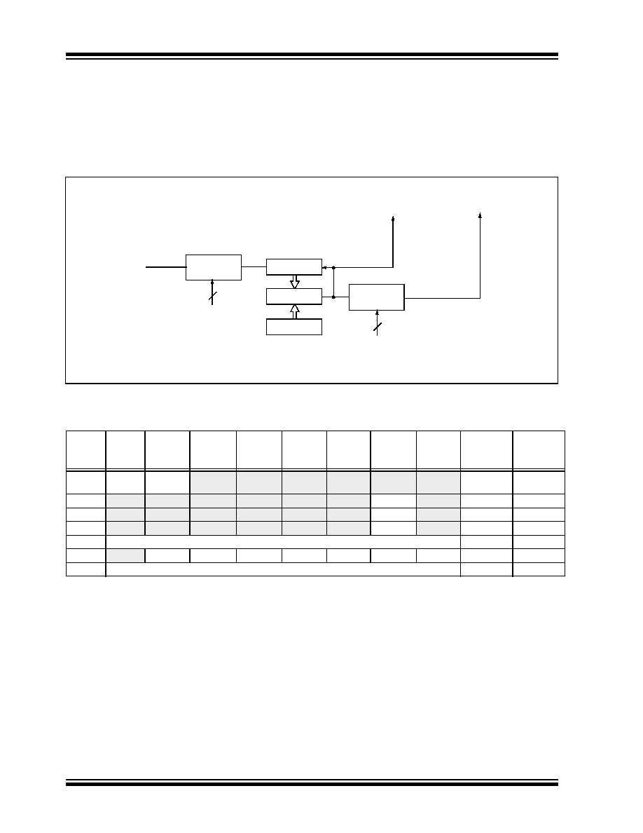
The Timer2 module has an 8-bit period register, PR2.
Timer2 increments from 00h until it matches PR2 and
then resets to 00h on the next increment cycle. PR2 is
a readable and writable register. The PR2 register is
initialized to FFh upon RESET.
12.3
Output of TMR2
The output of TMR2 (before the postscaler) is a clock
input to the Synchronous Serial Port module, which
optionally uses it to generate the shift clock.
FIGURE 12-1:
TIMER2 BLOCK DIAGRAM
TABLE 12-1:
REGISTERS ASSOCIATED WITH TIMER2 AS A TIMER/COUNTER
Comparator
TMR2
Sets Flag
TMR2
Output(1)
RESET
Postscaler
Prescaler
PR2
2
FOSC/4
1:1
1:16
1:1, 1:4, 1:16
EQ
4
bit TMR2IF
Note 1: TMR2 register output can be software selected by the SSP Module as a baud clock.
to
TOUTPS3:TOUTPS0
T2CKPS1:T2CKPS0
Name
Bit 7
Bit 6
Bit 5
Bit 4
Bit 3
Bit 2
Bit 1
Bit 0
Value on
POR, BOR
Value on
all other
RESETS
INTCON
GIE/
GIEH
PEIE/
GIEL
TMR0IE
INT0IE
RBIE
TMR0IF
INT0IF
RBIF
0000 000x
0000 000u
PIR1
—
ADIF
RCIF
TXIF
SSPIF
CCP1IF
TMR2IF
TMR1IF
-000 0000
PIE1
—
ADIE
RCIE
TXIE
SSPIE
CCP1IE
TMR2IE
TMR1IE
-000 0000
IPR1
—
ADIP
RCIP
TXIP
SSPIP
CCP1IP
TMR2IP
TMR1IP
-000 0000
TMR2
Timer2 Module’s Register
0000 0000
T2CON
—
TOUTPS3 TOUTPS2 TOUTPS1 TOUTPS0 TMR2ON
T2CKPS1
T2CKPS0 -000 0000 -000 0000
PR2
Timer2 Period Register
1111 1111
Legend: x = unknown, u = unchanged, - = unimplemented, read as '0'. Shaded cells are not used by the Timer2 module.
发布紧急采购,3分钟左右您将得到回复。
相关PDF资料
PIC18C658T-I/L
IC MCU OTP 16KX16 CAN 68PLCC
PIC18C658T-E/L
IC MCU OTP 16KX16 CAN 68PLCC
PIC16C925T-I/L
IC MCU OTP 4KX14 LCD DVR 68PLCC
PIC12F675-E/P
IC MCU CMOS 1K FLASH W/AD 8-DIP
PIC18C858T-E/L
IC MCU OTP 16KX16 CAN 84PLCC
PIC16F636-I/SL
IC PIC MCU FLASH 2KX14 14-SOIC
PIC18LC658T-I/L
IC MCU OTP 16KX16 CAN 68PLCC
PIC18LC801T-I/L
IC MCU ROMLESS A/D PWM 84PLCC
相关代理商/技术参数
PIC18C801T-I/PT
功能描述:8位微控制器 -MCU 2MB 1536 RAM 37I/O RoHS:否 制造商:Silicon Labs 核心:8051 处理器系列:C8051F39x 数据总线宽度:8 bit 最大时钟频率:50 MHz 程序存储器大小:16 KB 数据 RAM 大小:1 KB 片上 ADC:Yes 工作电源电压:1.8 V to 3.6 V 工作温度范围:- 40 C to + 105 C 封装 / 箱体:QFN-20 安装风格:SMD/SMT
PIC18C858-E/L
功能描述:8位微控制器 -MCU 32KB 1536 RAM 68I/O RoHS:否 制造商:Silicon Labs 核心:8051 处理器系列:C8051F39x 数据总线宽度:8 bit 最大时钟频率:50 MHz 程序存储器大小:16 KB 数据 RAM 大小:1 KB 片上 ADC:Yes 工作电源电压:1.8 V to 3.6 V 工作温度范围:- 40 C to + 105 C 封装 / 箱体:QFN-20 安装风格:SMD/SMT
PIC18C858-E/PT
功能描述:8位微控制器 -MCU 32KB 1536 RAM 68I/O RoHS:否 制造商:Silicon Labs 核心:8051 处理器系列:C8051F39x 数据总线宽度:8 bit 最大时钟频率:50 MHz 程序存储器大小:16 KB 数据 RAM 大小:1 KB 片上 ADC:Yes 工作电源电压:1.8 V to 3.6 V 工作温度范围:- 40 C to + 105 C 封装 / 箱体:QFN-20 安装风格:SMD/SMT
PIC18C858EPT
制造商:MICRO CHIP 功能描述:New
PIC18C858-I/L
功能描述:8位微控制器 -MCU 32KB 1536 RAM 68I/O RoHS:否 制造商:Silicon Labs 核心:8051 处理器系列:C8051F39x 数据总线宽度:8 bit 最大时钟频率:50 MHz 程序存储器大小:16 KB 数据 RAM 大小:1 KB 片上 ADC:Yes 工作电源电压:1.8 V to 3.6 V 工作温度范围:- 40 C to + 105 C 封装 / 箱体:QFN-20 安装风格:SMD/SMT
PIC18C858-I/PT
功能描述:8位微控制器 -MCU 32KB 1536 RAM 68I/O RoHS:否 制造商:Silicon Labs 核心:8051 处理器系列:C8051F39x 数据总线宽度:8 bit 最大时钟频率:50 MHz 程序存储器大小:16 KB 数据 RAM 大小:1 KB 片上 ADC:Yes 工作电源电压:1.8 V to 3.6 V 工作温度范围:- 40 C to + 105 C 封装 / 箱体:QFN-20 安装风格:SMD/SMT
PIC18C858T-E/L
功能描述:8位微控制器 -MCU 40MHz 16K OTP RoHS:否 制造商:Silicon Labs 核心:8051 处理器系列:C8051F39x 数据总线宽度:8 bit 最大时钟频率:50 MHz 程序存储器大小:16 KB 数据 RAM 大小:1 KB 片上 ADC:Yes 工作电源电压:1.8 V to 3.6 V 工作温度范围:- 40 C to + 105 C 封装 / 箱体:QFN-20 安装风格:SMD/SMT
PIC18C858T-E/PT
功能描述:8位微控制器 -MCU 32KB 1536 RAM 68I/O RoHS:否 制造商:Silicon Labs 核心:8051 处理器系列:C8051F39x 数据总线宽度:8 bit 最大时钟频率:50 MHz 程序存储器大小:16 KB 数据 RAM 大小:1 KB 片上 ADC:Yes 工作电源电压:1.8 V to 3.6 V 工作温度范围:- 40 C to + 105 C 封装 / 箱体:QFN-20 安装风格:SMD/SMT